Project Overview
This project focuses on the comparative analysis, transistor sizing, and simulation verification of a Single-Stage Operational Amplifier and a Two-Stage Miller-Compensated Operational Amplifier. Both topologies were designed to meet strict target specifications using custom manual sizing workflows and validated inside Cadence Virtuoso using the Spectre simulation platform on the gpdk180 (180nm) technology node.
Project Team: Mithun Hari, Raghavan, Vijhay Valliappan, Thughilan • Institution: PSG College of Technology, Coimbatore
Architectural Block Topology
The system architectures process analog signals through an multi-stage layout configuration. The internal design leverages a high-precision input differential stage, intermediate cascaded gain blocks, optimized level shifters, and an output buffer network to maintain structural signal fidelity.
Comparative Performance Matrix
Dynamic simulation capture across both configurations reveals significant performance differentials and architectural trade-offs:
| Performance Parameter | 1-Stage Op-Amp | 2-Stage Op-Amp | Analysis & Insights |
|---|---|---|---|
| DC Differential Gain (Ad) | 40.80 dB | 59.85 dB | The 2-stage achieves nearly 20 dB higher gain due to cascaded amplification loops. |
| Common Mode Gain (Ac) | -47.30 dB | -36.80 dB | The 1-stage exhibits better raw common-mode signal suppression. |
| CMRR | 88.10 dB | 96.64 dB | The 2-stage achieves superior CMRR due to its massive differential gain advantage. |
| Gain Bandwidth (GBW) | 4.68 MHz | 30.29 MHz | The 2-stage offers an expanded frequency response sweep window. |
| Phase Margin (PM) | ≈89.5° | 47.25° | The 1-stage is unconditionally stable; the 2-stage trades PM for bandwidth extensions. |
| Slew Rate (SR) | 5.32 V/µs | 42.50 V/µs | The 2-stage handles large-signal transient switches significantly faster. |
Single-Stage Op-Amp Design
The single-stage architecture implements a dual-input balanced-output differential amplifier paired with active load current mirrors to maximize common-mode rejection and initial layout open-loop gain.
📐 Sizing & Aspect Ratios
- Differential Input Pair (M1, M2): W/L = 7
- Active Load Mirrors (M3, M4): W/L = 15
- Tail Current Mirrors (M5, M6): W/L = 13.67
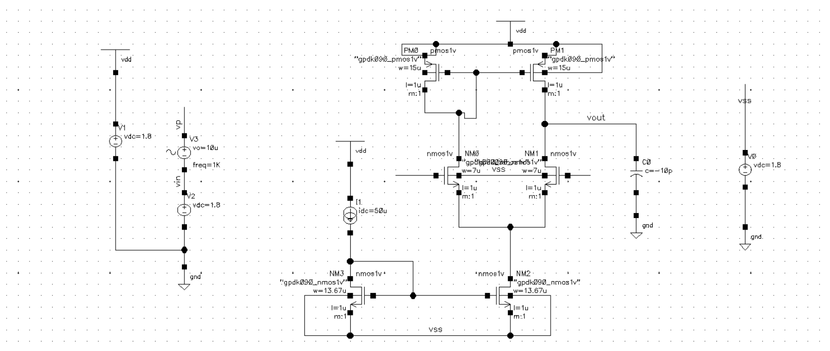
Figure 2: Schematic capture of the baseline single-stage architecture within Cadence Virtuoso.
📈 AC Characterization Waveforms
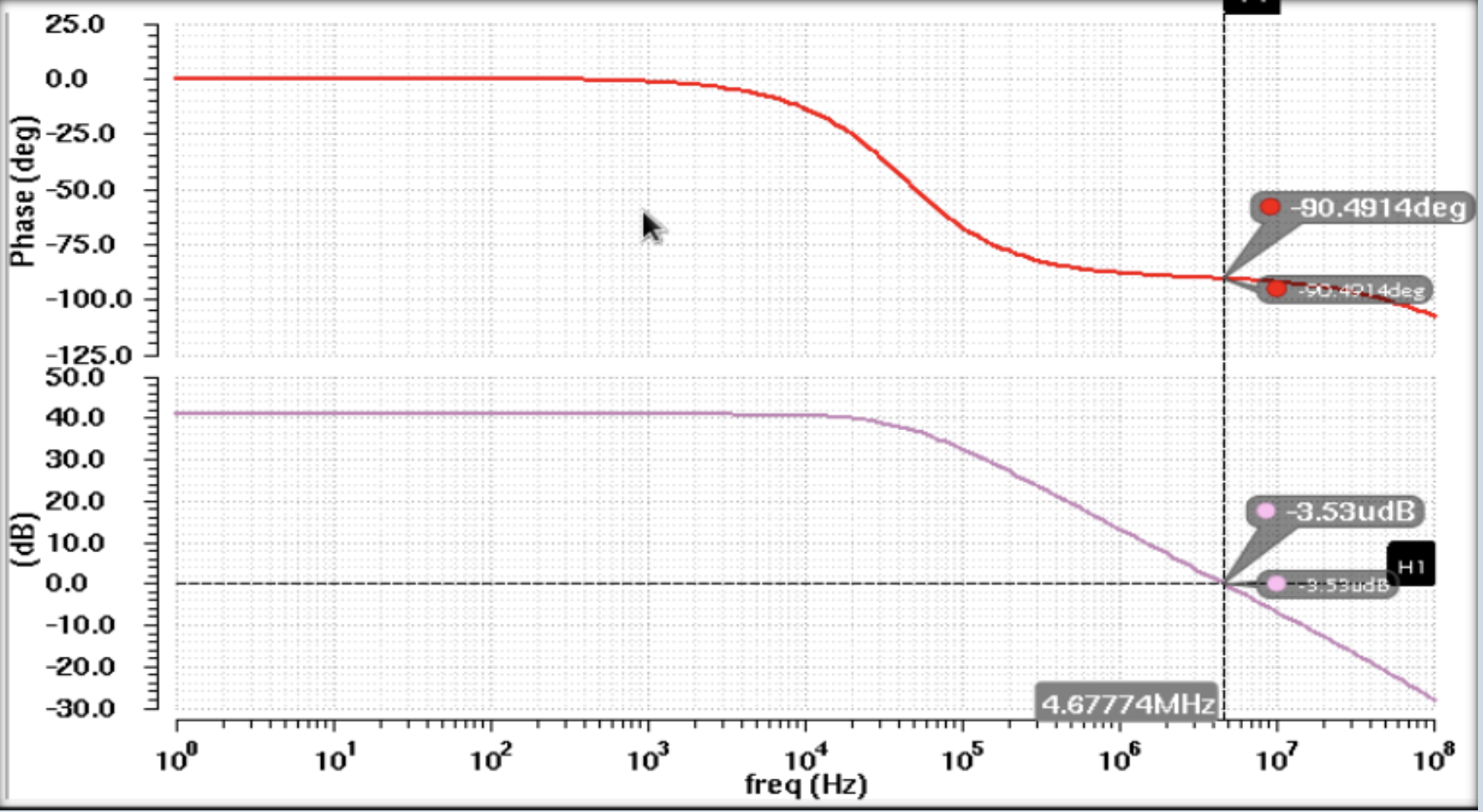
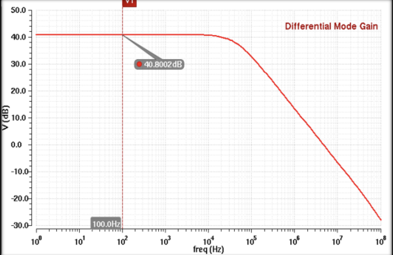
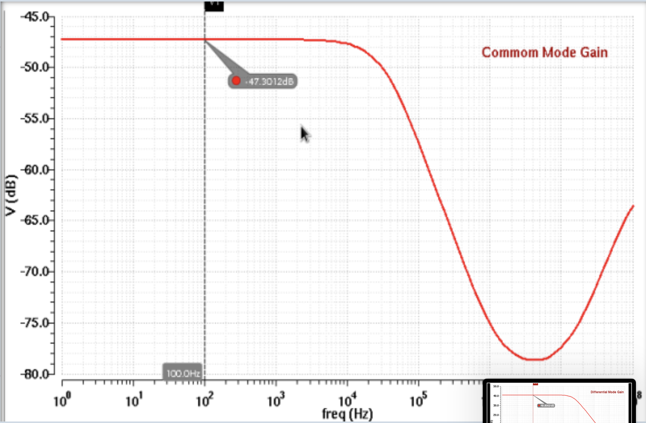
Figure 3: Unconditionally stable frequency sweeps for Phase, Differential, and Common-Mode parameters.
Two-Stage Op-Amp Design
The two-stage configuration splits voltage amplification into an initial input differential stage followed by a common-source output stage. Miller Compensation (Cc) and Pole-Splitting methodologies isolate dominant and non-dominant poles to maintain strict stability parameters under closed feedback loops.
📐 Sizing & Aspect Ratios
- Transistor Sizing Ratios: M1, M2 = 6 | M3, M4 = 8 | M5 = 124.56 | M6 = 31.14 | M7, M8 = 4
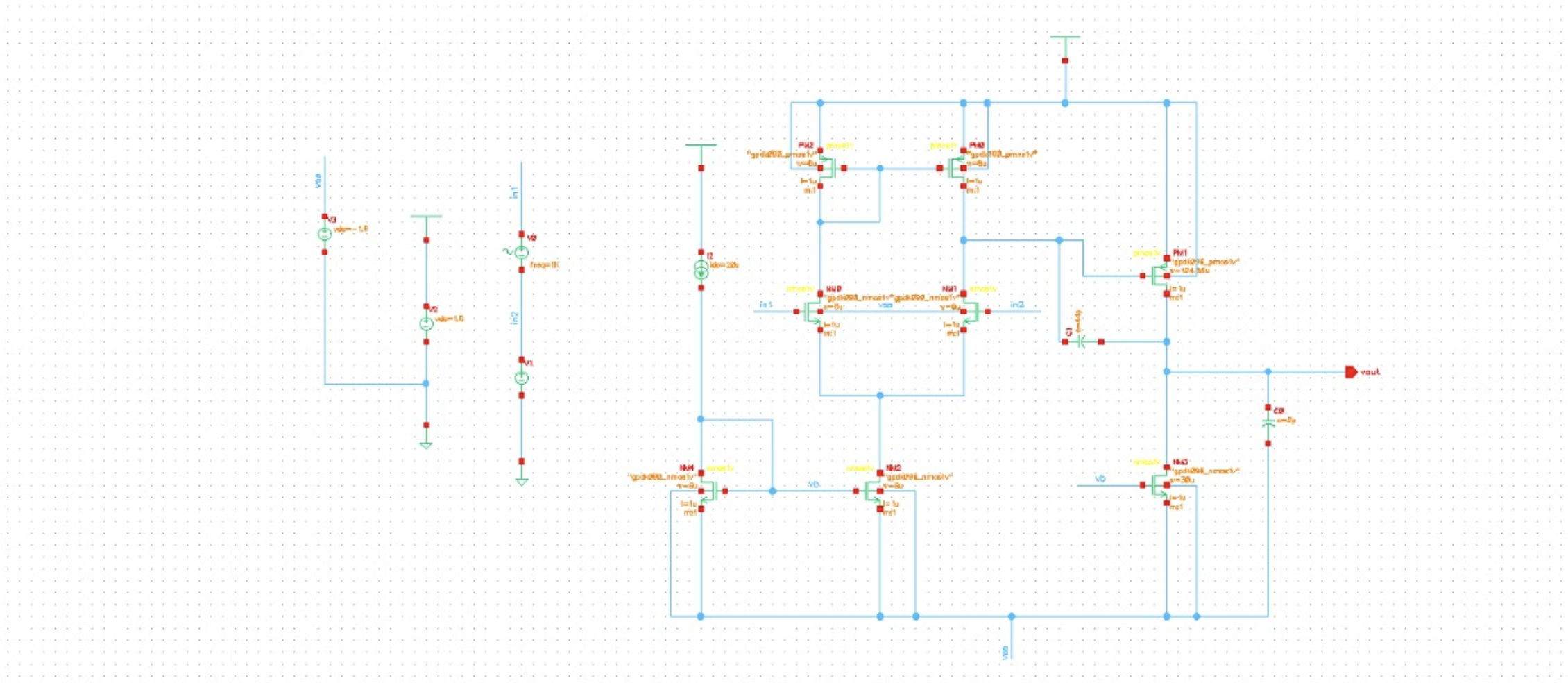
Figure 4: Expanded Two-Stage layout configuration with embedded Miller compensation networks.
📈 AC Characterization Waveforms
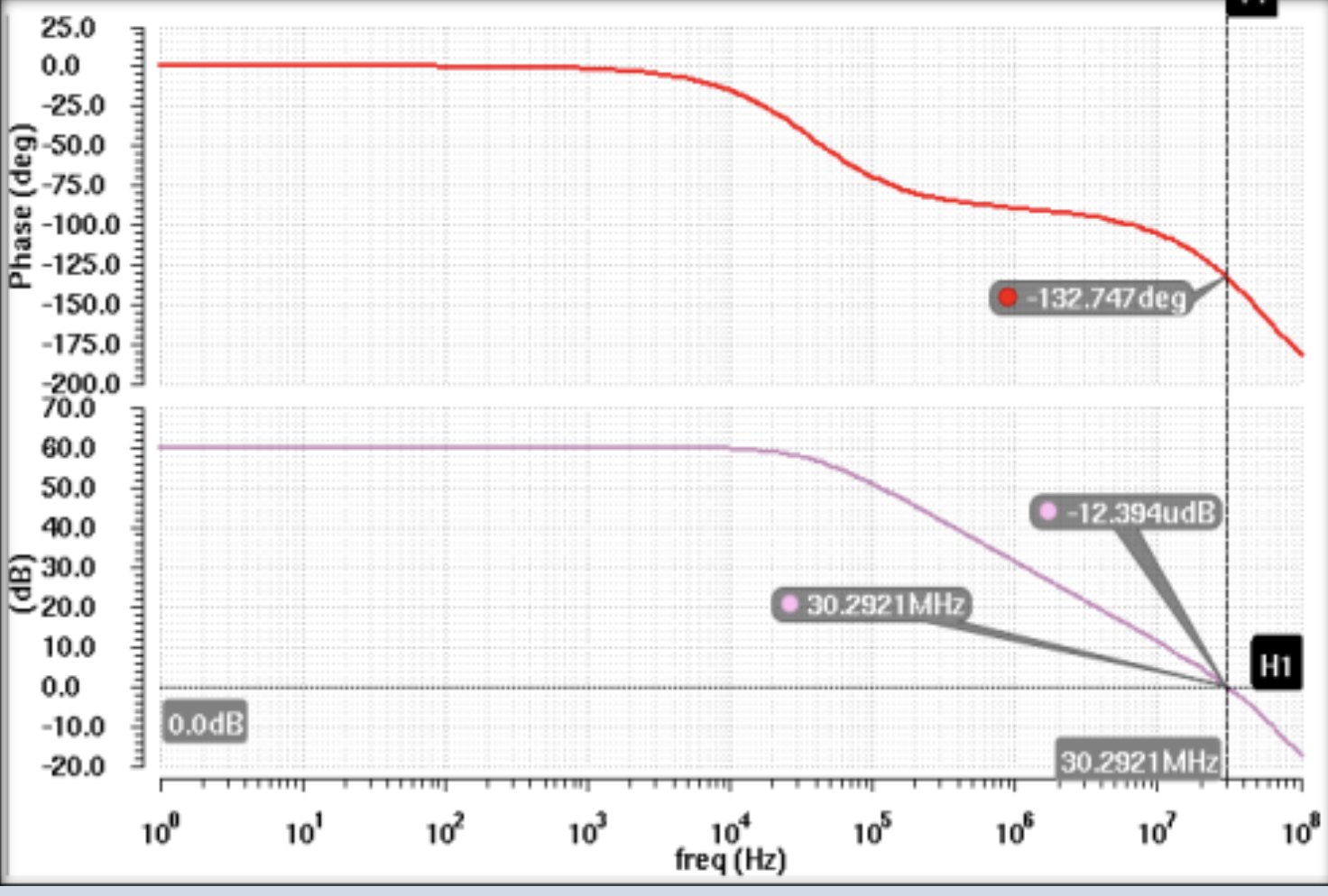
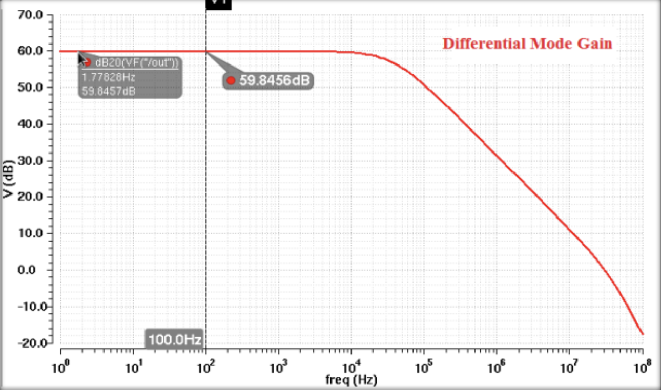
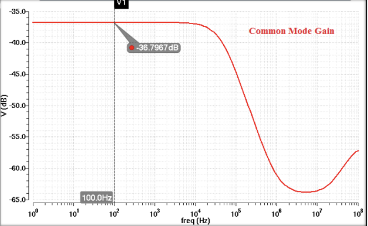
Figure 5: Closed-loop frequency plots demonstrating expanded Gain Bandwidth (GBW) and bounded phase margin tracking.
Key Engineering Takeaways
40.8 dB
1-Stage Open-Loop Gain
59.85 dB
2-Stage Cascaded Gain
30.29 MHz
Scaled Gain Bandwidth (GBW)
8x Accel
Transient Slew Rate Bootstrapping
The Gain-Stability Dilemma: The single-stage topology functions effectively as a single-pole system, yielding near-perfect stability ($PM \approx 89.5^\circ$) but bounding open-loop gain limits. Reconfiguring into a 2-stage architecture successfully boosts the open-loop gain by roughly $20\text{ dB}$ and scales the bandwidth execution boundaries while holding stable phase tracking above design constraints ($PM = 47.25^\circ$).
Design Infrastructure & Tooling
- Cadence Virtuoso: Transistor schematic capture, sizing matrix deployment, and multi-node parameter variation.
- Spectre Simulation Platform: Evaluation engine for AC frequency sweeps, Transient analysis, and Common-Mode performance matrices.
Note on Architecture Repository: Due to a routine server sweep on laboratory local workstations, the active schematic database directory instances were flushed. This portfolio block handles data storage validation, hosting the structural backups, design slides (FINAL Draft.pdf), and performance validation graphs generated across the design lifecycle.