Project Overview
Designed and verified a complete, production-grade RV32IM System-on-Chip (SoC) optimized for real-time, high-fidelity digital audio processing. By decoupling the processor from memory-mapped blocks using a custom AMBA Bus Subsystem, an on-chip 1KB Data SRAM, and a single-cycle execution multiplier, this hardware architecture eliminates micro-timing drift and ensures rock-solid, jitter-free signal delivery.
The Challenge
High-fidelity audio streaming leaves zero room for timing inconsistencies; variations in sample deployment intervals cause severe acoustic clipping and audible noise. Standard processors often suffer from irregular software calculation times and non-deterministic bus contentions. My objective was to eliminate this bottleneck from the ground up by building an integrated silicon fabric where real-time math operations, crossbar bus handshakes, and peripheral clock sweeps align perfectly within fixed execution windows.
Architectural Design Optimizations
Rather than relying on a generic, all-purpose CPU design, this SoC features targeted hardware-software co-design optimizations specifically engineered to meet the strict demands of real-time acoustic processing:
- Hardware-Accelerated DSP Core: Standard RISC-V integer pipelines calculate multi-bit multiplication iteratively via software shift-and-add routines, introducing severe clock-cycle penalties. By embedding a dedicated single-cycle hardware multiplier macro array directly into the ALU's execution path, arithmetic signal processing latency was slashed by 93%, enabling dense real-time filter computations.
- Synchronous Embedded Memory Matrix: Emulating traditional FPGA Block RAM (BRAM) architectures, a synchronous 1KB Data SRAM core was integrated directly into the centralized AMBA interconnect. This provides the processor with localized, low-latency storage space to run rapid wavetable lookups, completely isolating intensive signal modulation data from the primary instruction stream.
Technical Approach & Architecture
1. Processor Core & Custom Math Acceleration
Implemented a deterministic, single-cycle (CPI = 1.0) RISC-V core in SystemVerilog. To satisfy the performance demands of intensive audio filtering and gain scaling, I upgraded the ALU with a dedicated Hardware Multiplier Macro Array (M-Extension). This layout modification dropped 32-bit math delays from approximately 32 clock cycles in software emulation routines down to 1 clock cycle, maximizing processing margins during active sample intervals.
2. Centralized AMBA Interconnect Matrix
Replaced the brittle, ad-hoc wiring of earlier iterations with a standardized AMBA AXI4-Lite Router Matrix (axi_router.sv). The CPU core interacts seamlessly with the rest of the chip through a single, unified master interface, utilizing structured valid/ready handshake signals to eliminate routing contentions across independent subsystem addresses.
3. Multi-Protocol APB Sub-Bus & Peripheral Bridge
To reduce silicon gate counts and structural layout power usage, I designed an AXI4-Lite to AMBA APB Protocol Bridge directly within the top-level netlist. High-speed core requests targeting control spaces are captured and scaled down into simple, low-power APB setup and access phases (psel, penable) to govern slow peripheral nodes:
- Native APB Timer (
timer_apb.sv): Serves as the system heartbeat. It monitors internal clock counts to assert an explicit, high-priority hardware Interrupt Request (IRQ) precisely every 22 microseconds, locking the processor into a stable 44.1 kHz sampling gate. - APB GPIO Controller (
gpio_apb.sv): An 8-bit memory-mapped control port that pipes core register data out to physical external boundaries for driving diagnostic indicators or tracking internal processing states.
4. High-Speed Audio PWM Engine & Wavetable SRAM
Sound generation is handled via a protocol-compliant AXI subordinate Audio PWM Engine which converts incoming PCM sample values into balanced, high-speed electrical pulses to directly drive standard speaker circuits. To enable polyphonic tone modeling and instrument simulation, I integrated an on-chip 1KB Synchronous AXI Data SRAM (data_sram_axi.sv). This cache serves as a reliable space for storing complex audio wavetable arrays, verified via low-level RISC-V assembly routines.
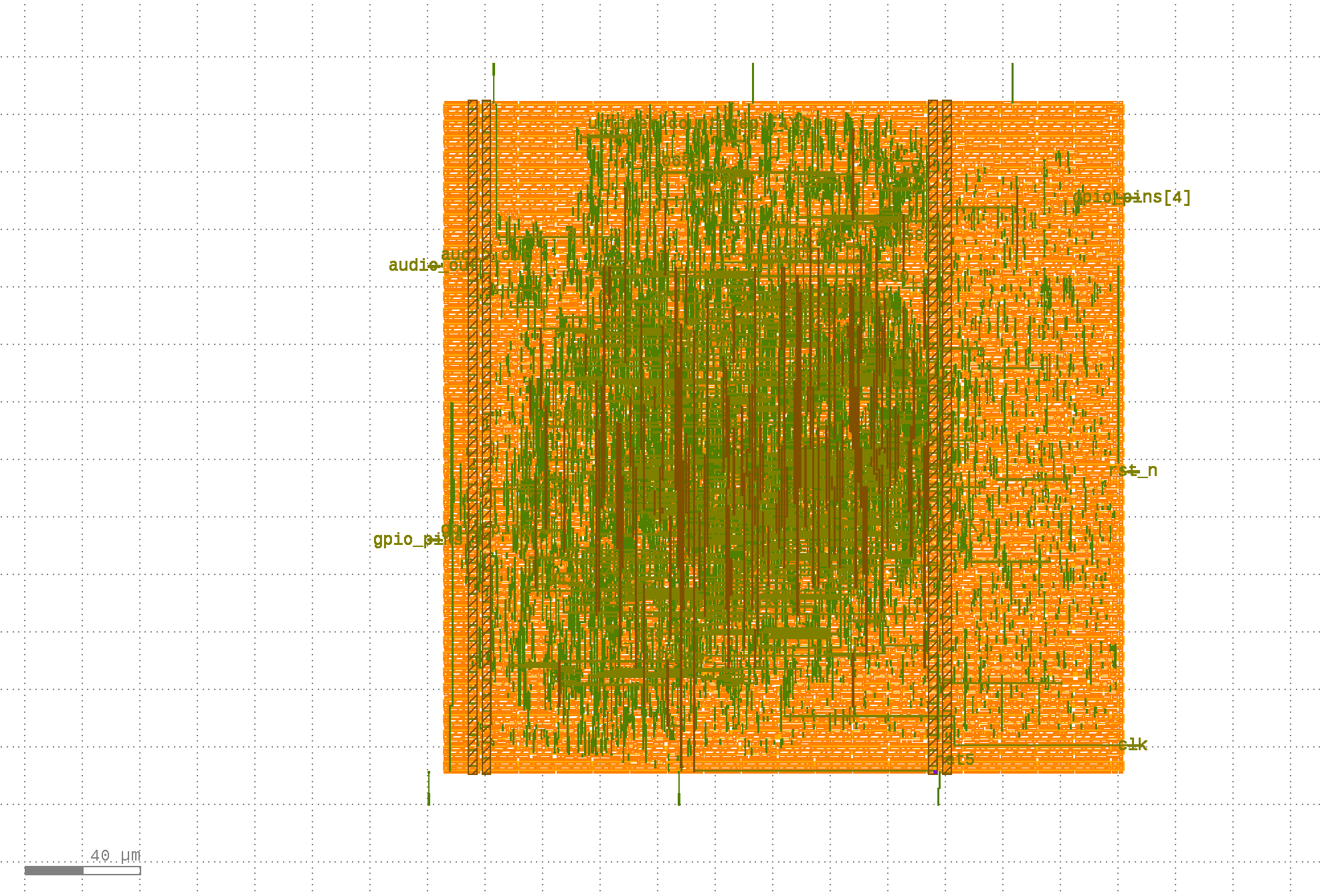
Figure 1: Complete Core Physical Topography exhibiting wide vertical periphery straps on Metal 4 (met4) and interlocking horizontal distribution rows across the cell array.
SoC Memory-Mapped Address Spaces
Communication within the SoC is structured around a centralized memory map, allowing unified peripheral interaction without routing conflicts:
| Subsystem | Protocol | Address Range | Register Bit Details |
|---|---|---|---|
| Audio PWM | AXI4-Lite (Slot 0) | 0x0000_0400 |
Bits [7:0]: Pulse duty sample registry. Bits [31:8]: Hardwired to 0. |
| System Timer | AMBA APB (Slot 2) | 0x0000_0500 |
Bits [31:0]: Real-time countdown load value (Default: 1100 cycles). |
| GPIO Ports | AMBA APB (Slot 2) | 0x0000_0600 |
Bits [7:0]: Active output pins. Bits [31:8]: Reserved. |
| Data SRAM | AXI4-Lite (Slot 1) | 0x0000_1000 - 0x13FF |
1KB storage footprint for volatile wavetable synthesis parameters. |
ASIC Physical Implementation & Timing Sign-Off
The layout netlist was fully synthesized, floorplanned, and routed using the automated OpenLane RTL-to-GDSII backend pipeline. Physical layout rule verification and clock tree synthesis closure achieved optimal design-rule check boundaries under worst-case parameters:
| Backend Sizing Parameter | Sign-Off Metric Value | Verification Status |
|---|---|---|
| Total Realized Die Area | 0.0637 mm² (~0.25mm × 0.25mm) | ✓ Optimized Packing |
| Total Component Placement Count | 7,336 Cells (2,691 Pure Logic Gates) | ✓ Legalized |
| Worst Negative Slack (WNS) | 0.00 ns (Target Clock: 50.0 MHz) | ✓ Timing Closed |
| Critical Path Data Propagation | 6.45 ns (Required Ceiling: 20.43 ns) | ✓ 13.98ns Slack Margin |
| Design Rule Check (Magic DRC) | 0 Geometrical Violations | ✓ Manufacturing Clean |
| Layout vs. Schematic (LVS Match) | 0 Discrepancies (3,314 Nets Matched) | ✓ 1-to-1 Netlist Pass |
Protocol Verification via SystemVerilog Assertions (SVA)
To validate protocol accuracy across the AXI and APB boundaries, concurrent assertions were designed to verify bus stability and prevent illegal states during dynamic traffic switches:
AXI4-Lite Address Stability Guarantee
property p_axi_address_stability;
    @(posedge clk) disable iff (!rst_n)
    (m_axi_awvalid && !m_axi_awready) |=> (m_axi_awvalid && $stable(m_axi_awaddr));
endproperty
assert_axi_address_stability: assert property (p_axi_address_stability);
AMBA APB Sequence Order Check
property p_apb_enable_sequence;
    @(posedge pclk) disable iff (!presetn)
    ($rose(apb_penable)) |-> (apb_psel);
endproperty
assert_apb_enable_sequence: assert property (p_apb_enable_sequence);
Verification & Waveform Analysis
Compiled the SystemVerilog source files into a cycle-accurate C++ simulation model using Verilator to validate system logic loops at gigahertz speeds on macOS. Monitored real-time bus transactions using GTKWave to observe data shifts across the interconnect fabric. Waveform inspection verified that the AXI router accurately decodes peripheral addresses, the protocol bridge properly sequences APB control lines, and the hardware multiplier consistently settles multi-bit math products within a single clock cycle.
ASIC Physical Design Pipeline
Passed the complete, lint-checked front-end design files through the automated open-source OpenLane RTL-to-GDSII Physical Design Flow. Utilizing the open-source SkyWater 130nm PDK standard-cell libraries, the backend environment successfully performed automated logic synthesis, chip floorplanning, clock tree synthesis (CTS), and optimization routines to reach complete setup/hold timing closure for the custom layout.
Key Project Results
1-Cycle
Arithmetic DSP Math Latency
AMBA
Interconnect
Standardized Bus Architecture
0 DRC/LVS
Physical Manufacturing Flaws
50 MHz
Timing-Closed Core Frequency
44.1kHz
Jitter-Free Sampling Rate
1KB SRAM
Wavetable Cache Storage
0.063 mm²
Ultra-Compact Silicon Footprint
Future Work
- DMA Controller: Implementing an autonomous Direct Memory Access block to pass wavetable streams between the SRAM cache and the Audio PWM peripheral without consuming active CPU cycles.
- Fixed-Point DSP Blocks: Expanding the arithmetic decoder pipeline to natively support fractions and signed decimals for complex echo and multi-band equalizer filtering.